Publications
For the most up to date list of publications, please see Google Scholar
Multi-objective optimization of building integrated photovoltaic solar shades
Seyedsoroush Sadatifar, Eric Johlin
Solar Energy 242, 191 (2022)

Building-integrated photovoltaic (BIPV) systems allow solar panels to perform additional functions beyond energy generation for buildings, such as regulating interior lighting conditions and incoming radiative heat. However, optimizations of BIPV solar shades generally do not consider all of these factors, instead often focusing on power production alone. In this work, we explore a design framework for optimizing the configuration of BIPV shading devices to maximize a combination of power generation, interior daylighting quality, and radiative heating and cooling loads. This is applied to a simple room in five different locations and climates, as well as a case study of an office building. The low computational cost of this model allows for the full mapping of the influence of all design parameters on the value of the system, while demonstrating less than 7% error in predicting the performance of a benchmark experimental system. It is observed that the location and building geometry have significant influences on the relative values of heat, daylighting, and power production, with the overall combined value varying by up to 40% between the compared climates. The optimal design in many locations depend on user preferences as well, with many efficient solutions possible for varying trade-offs between the values of natural light vs. energy savings (a difference of up to 50%), as well as the system upfront cost vs. performance, further reinforcing the importance of tailored building-specific design for BIPV solar shades.
Nanophotonic color splitters for high-efficiency imaging
Eric Johlin
iScience 24, 102268 (2021)

Standard color imaging utilizes absorptive filter arrays to achieve spectral sensitivity. However, this leads to ∼2/3 of incident light being lost to filter absorption. Instead, splitting and redirecting light into spatially separated pixels avoids these absorptive losses. Herein we investigate the inverse design and performance of a new type of splitter which can be printed from a single material directly on top of a sensor surface and are compatible with 800 nm sensor pixels, thereby providing drop-in replacements for color filters. Two-dimensional structures with as few as four layers significantly improve fully color-corrected imaging performance over standard filters, with lower complexity. Being fully dielectric, these splitters additionally allow color-correction to be foregone, increasing the photon transmission efficiency to over 80%, even for sensors with fill-factors of 0.5. Performance further increases with fully 3D structures, improving light sensitivity in color-corrected imaging by a factor of 4 when compared to filters alone.
Integrating Sphere Fourier Microscopy of Highly Directional Emission
Julia S Van Der Burgt, Christian D Dieleman, Eric Johlin, Jaco J Geuchies, Arjan J Houtepen, Bruno Ehrler, Erik C Garnett
ACS Photonics 8, 1143 (2021)

Standard color imaging utilizes absorptive filter arrays to achieve spectral sensitivity. However, this leads to ∼2/3 of incident light being lost to filter absorption. Instead, splitting and redirecting light into spatially separated pixels avoids these absorptive losses. Herein we investigate the inverse design and performance of a new type of splitter which can be printed from a single material directly on top of a sensor surface and are compatible with 800 nm sensor pixels, thereby providing drop-in replacements for color filters. Two-dimensional structures with as few as four layers significantly improve fully color-corrected imaging performance over standard filters, with lower complexity. Being fully dielectric, these splitters additionally allow color-correction to be foregone, increasing the photon transmission efficiency to over 80%, even for sensors with fill-factors of 0.5. Performance further increases with fully 3D structures, improving light sensitivity in color-corrected imaging by a factor of 4 when compared to filters alone.
Broadband highly directive 3D nanophotonic lenses
Eric Johlin, Sander A Mann, Sachin Kasture, A Femius Koenderink, Erik C Garnett
Nature Communications 9, 4742 (2018)
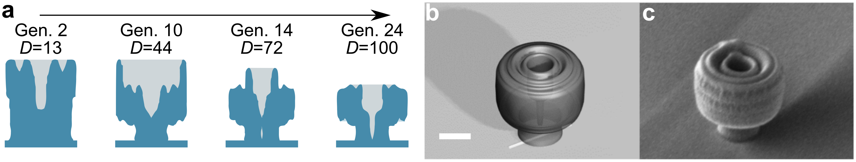
Controlling the directivity of emission and absorption at the nanoscale holds great promise for improving the performance of optoelectronic devices. Previously, directive structures have largely been centered in two categories—nanoscale antennas, and classical lenses. Herein, we utilize an evolutionary algorithm to design 3D dielectric nanophotonic lens structures leveraging both the interference-based control of antennas and the broadband operation of lenses. By sculpting the dielectric environment around an emitter, these nanolenses achieve directivities of 101 for point-sources, and 67 for finite-source nanowire emitters; 3× greater than that of a traditional spherical lens with nearly constant performance over a 200 nm wavelength range. The nanolenses are experimentally fabricated on GaAs nanowires, and characterized via photoluminescence Fourier microscopy, with an observed beaming half-angle of 3.5° and a measured directivity of 22. Simulations attribute the main limitation in the obtained directivity to imperfect alignment of the nanolens to the nanowire beneath.
Nanoscale back contact perovskite solar cell design for improved tandem efficiency
GWP Adhyaksa, E Johlin, EC Garnett
Nano Letters 17, 5206 (2017)
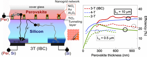
Tandem photovoltaics, combining absorber layers with two distinct band gap energies into a single device, provide a practical solution to reduce thermalization losses in solar energy conversion. Traditionally, tandem devices have been assembled using two-terminal (2-T) or four-terminal (4-T) configurations; the 2-T limits the tandem performance due to the series connection requiring current matching, while the standard 4-T configuration requires at least three transparent electrical contacts, which reduce the total collected power due to unavoidable parasitic absorption. Here, we introduce a novel architecture based on a nanoscale back-contact for a thin-film top cell in a three terminal (3-T) configuration. Using coupled optical–electrical modeling, we optimize this architecture for a planar perovskite-silicon tandem, highlighting the roles of nanoscale contacts to reduce the required perovskite electronic quality. For example, with an 18% planar silicon base cell, the 3-T back contact design can reach a 32.9% tandem efficiency with a 10 μm diffusion length perovskite material. Using the same perovskite quality, the 4-T and 2-T configurations only reach 30.2% and 24.8%, respectively. We also confirm that the same 3-T efficiency advantage applies when using 25% efficient textured silicon base cells, where the tandems reach 35.2% and 32.8% efficiency for the 3-T, and 4-T configurations, respectively. Furthermore, because our design is based on the individual subcells being back-contacted, further improvements can be readily made by optimizing the front surface, which is left free for additional antireflective coating, light trapping, surface passivation, and photoluminescence outcoupling enhancements.
3D multi-energy deconvolution electron microscopy
Michiel de Goede, Eric Johlin, Beniamino Sciacca, Faysal Boughorbel and Erik C. Garnett
Nanoscale 9, 684 (2017)
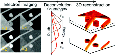
Three-dimensional (3D) characterization of nanomaterials is traditionally performed by either cross-sectional milling with a focused ion beam (FIB), or transmission electron microscope tomography. While these techniques can produce high quality reconstructions, they are destructive, or require thin samples, often suspended on support membranes. Here, we demonstrate a complementary technique allowing non-destructive investigation of the 3D structure of samples on bulk substrates. This is performed by imaging backscattered electron (BSE) emission at multiple primary beam energies – as the penetration depth of primary electrons is proportional to the beam energy, depth information can be obtained through variations in the beam acceleration. The detected signal however consists of a mixture of the penetrated layers, meaning the structure's three-dimensional geometry can only be retrieved after deconvolving the BSE emission profile from the observed BSE images. This work demonstrates this novel approach by applying a blind source separation deconvolution algorithm to multi-energy acquired BSE images. The deconvolution can thereby allow a 3D reconstruction to be produced from the acquired images of an arbitrary sample, showing qualitative agreement with the true depth structure, as verified through FIB cross-sectional imaging.
Super-resolution imaging of light–matter interactions near single semiconductor nanowires
Eric Johlin, Jacopo Solari, Sander A. Mann, Jia Wang, Thomas S. Shimizu & Erik C. Garnett
Nature Communications 7, 13950 (2016)
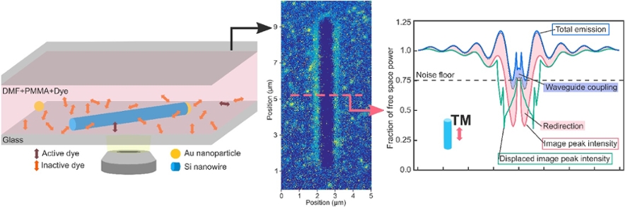
Nanophotonics is becoming invaluable for an expanding range of applications, from controlling the spontaneous emission rate and the directionality of quantum emitters, to reducing material requirements of solar cells by an order of magnitude. These effects are highly dependent on the near field of the nanostructure, which constitutes the evanescent fields from propagating and resonant localized modes. Although the interactions between quantum emitters and nanophotonic structures are increasingly well understood theoretically, directly imaging these interactions experimentally remains challenging. Here we demonstrate a photoactivated localization microscopy-based technique to image emitter-nanostructure interactions. For a 75 nm diameter silicon nanowire, we directly observe a confluence of emission rate enhancement, directivity modification and guided mode excitation, with strong interaction at scales up to 13 times the nanowire diameter. Furthermore, through analytical modelling we distinguish the relative contribution of these effects, as well as their dependence on emitter orientation.
Nanohole Structuring for Improved Performance of Hydrogenated Amorphous Silicon Photovoltaics
Eric Johlin, Ahmed Al-Obeidi, Gizem Nogay, Michael Stuckelberger, Tonio Buonassisi, Jeffrey C Grossman
ACS Applied Materials & Interfaces 8, 15169 (2016)
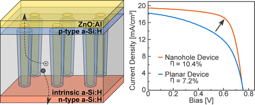
While low hole mobilities limit the current collection and efficiency of hydrogenated amorphous silicon (a-Si:H) photovoltaic devices, attempts to improve mobility of the material directly have stagnated. Herein, we explore a method of utilizing nanostructuring of a-Si:H devices to allow for improved hole collection in thick absorber layers. This is achieved by etching an array of 150 nm diameter holes into intrinsic a-Si:H and then coating the structured material with p-type a-Si:H and a conformal zinc oxide transparent conducting layer. The inclusion of these nanoholes yields relative power conversion efficiency (PCE) increases of ∼45%, from 7.2 to 10.4% PCE for small area devices. Comparisons of optical properties, time-of-flight mobility measurements, and internal quantum efficiency spectra indicate this efficiency is indeed likely occurring from an improved collection pathway provided by the nanostructuring of the devices. Finally, we estimate that through modest optimizations of the design and fabrication, PCEs of beyond 13% should be obtainable for similar devices.
A Framework for Process-to-Module Modeling of a-Si/c-Si (HIT) Heterojunction Solar Cells to Investigate the Cell-to-Module Efficiency Gap
Raghu Vamsi Krishna Chavali, Eric C Johlin, Jeffery Lynn Gray, Tonio Buonassisi, Muhammad Ashraful Alam
IEEE Journal of Photovoltaics 6, 875 (2016)
The cell-to-module efficiency gap observed in a-Si/c-Si heterojunction solar cells is a key challenge to the broad adoption of this technology. To systematically address this issue, we describe an end-to-end modeling framework to explore the implications of process and device variations at the module level. First, a process model is developed to connect the a-Si deposition parameters to the material properties. Next, a physics-based device model is presented; the model uses the thermionic emission/diffusion theory to capture the essential features of photocurrent and diode injection current. Using the process and device models, the effects of process conditions on cell performance are explored. Finally, the performance of the module, as a function of device and process parameters, is explored to establish the cell-to-module efficiency gap. The insights developed through this process-to-module modeling framework will help close the cell-to-module efficiency gap of this commercially promising technology.
Stress effects on the Raman spectrum of an amorphous material: Theory and experiment on a-Si: H
David A Strubbe, Eric C Johlin, Timothy R Kirkpatrick, Tonio Buonassisi, Jeffrey C Grossman
Physical Review B 92, 241202 (2016)
Strain in a material induces shifts in vibrational frequencies. This phenomenon is a probe of the nature of the vibrations and interatomic potentials and can be used to map local stress/strain distributions via Raman microscopy. This method is standard for crystalline silicon devices, but due to the lack of calibration relations, it has not been applied to amorphous materials such as hydrogenated amorphous silicon (a-Si:H), a widely studied material for thin-film photovoltaic and electronic devices. We calculated the Raman spectrum of a-Si:H ab initio under different strains ε and found peak shifts Δω=(−460±10cm−1)Trε. This proportionality to the trace of the strain is the general form for isotropic amorphous vibrational modes, as we show by symmetry analysis and explicit computation. We also performed Raman measurements under strain and found a consistent coefficient of −510±120cm−1. These results demonstrate that a reliable calibration for the Raman/strain relation can be achieved even for the broad peaks of an amorphous material, with similar accuracy and precision as for crystalline materials.
A 2-terminal perovskite/silicon multijunction solar cell enabled by a silicon tunnel junction
Jonathan P Mailoa, Colin D Bailie, Eric C Johlin, Eric T Hoke, Austin J Akey, William H Nguyen, Michael D McGehee, Tonio Buonassisi
Applied Physics Letters 106, 121105 (2015)
With the advent of efficient high-bandgap metal-halide perovskite photovoltaics, an opportunity exists to make perovskite/silicon tandem solar cells. We fabricate a monolithic tandem by developing a silicon-based interband tunnel junction that facilitates majority-
carrier charge recombination between the perovskite and silicon sub-cells. We demonstrate a 1 cm2 2-terminal monolithic perovskite/silicon multijunction solar cell with a V OC as high as 1.65 V. We achieve a stable 13.7% power conversion efficiency with the perovskite as the current-limiting sub-cell, and identify key challenges for this device architecture to reach efficiencies over 25%.
Hole-mobility-limiting atomic structures in hydrogenated amorphous silicon
Eric Johlin, CB Simmons, Tonio Buonassisi, Jeffrey C Grossman
Physical Review B 90, 104103 (2014)
Abstract Low hole mobility currently limits the efficiency of amorphous silicon photovoltaic devices. We explore three possible phenomena contributing to this low mobility: coordination defects, self-trapping ionization displacement defects, and lattice expansion allowing for hole wave-function delocalization. Through a confluence of experimental and first-principles investigations, we demonstrate the fluidity of the relative prevalence of these defects as film stress and hydrogen content are modified, and that the mobility of a film is governed by an interplay between various defect types.
Grain boundary engineering for improved thin silicon photovoltaics
Rajamani Raghunathan, Eric Johlin, Jeffrey C Grossman
Nano Letters 14, 4943 (2014)
In photovoltaic devices, the bulk disorder introduced by grain boundaries (GBs) in polycrystalline silicon is generally considered to be detrimental to the physical stability and electronic transport of the bulk material. However, at the extremum of disorder, amorphous silicon is known to have a beneficially increased band gap and enhanced optical absorption. This study is focused on understanding and utilizing the nature of the most commonly encountered Σ3 GBs, in an attempt to balance incorporation of the advantageous properties of amorphous silicon while avoiding the degraded electronic transport of a fully amorphous system. A combination of theoretical methods is employed to understand the impact of ordered Σ3 GBs on the material properties and full-device photovoltaic performance.
Origins of hole traps in hydrogenated nanocrystalline and amorphous silicon revealed through machine learning
Tim Mueller, Eric Johlin, Jeffrey C Grossman
Physical Review B 89, 115202 (2014)
Genetic programming is used to identify the structural features most strongly associated with hole traps in hydrogenated nanocrystalline silicon with very low crystalline volume fraction. The genetic programming algorithm reveals that hole traps are most strongly associated with local structures within the amorphous region in which a single hydrogen atom is bound to two silicon atoms (bridge bonds), near fivefold coordinated silicon (floating bonds), or where there is a particularly dense cluster of many silicon atoms. Based on these results, we propose a mechanism by which deep hole traps associated with bridge bonds may contribute to the Staebler-Wronski effect.Origins of structural hole traps in hydrogenated amorphous silicon
Eric Johlin, Lucas K Wagner, Tonio Buonassisi, Jeffrey C Grossman
Physical Review Letters 110, 146805 (2013)
The inherently disordered nature of hydrogenated amorphous silicon (a-Si: H) obscures the influence of atomic features on the trapping of holes. To address this, we have created a set of over two thousand ab initio structures of a-Si: H and explored the influence of geometric factors on the occurrence of deep hole traps using density-functional theory. Statistical analysis of the relative contribution of various structures to the trap distribution shows that floating bonds and ionization-induced displacements correlate most strongly with
hole traps in our ensemble.
Structural origins of intrinsic stress in amorphous silicon thin films
Eric Johlin, Nouar Tabet, Sebastián Castro-Galnares, Amir Abdallah, Mariana I Bertoni, Tesleem Asafa, Jeffrey C Grossman, Syed Said, Tonio Buonassisi
Physical Review B 85, 075202 (2012)
Hydrogenated amorphous silicon (a-Si:H) refers to a broad class of atomic configurations, sharing a lack of long-range order, but varying significantly in material properties, including optical constants, porosity, hydrogen content, and intrinsic stress. It has long been known that deposition conditions affect microstructure, but much work remains to uncover the correlation between these parameters and their influence on electrical, mechanical, and optical properties critical for high-performance a-Si:H photovoltaic devices. We synthesize and augment several previous models of deposition phenomena and ion bombardment, developing a refined model correlating plasma-enhanced chemical vapor deposition conditions (pressure and discharge power and frequency) to the development of intrinsic stress in thin films. As predicted by the model presented herein, we observe that film compressive stress varies nearly linearly with bombarding ion momentum and with a (−1/4) power dependence on deposition pressure, that tensile stress is proportional to a reduction in film porosity, and the net film intrinsic stress results from a balance between these two forces. We observe the hydrogen-bonding configuration to evolve with increasing ion momentum, shifting from a void-dominated configuration to a silicon-monohydride configuration. Through this enhanced understanding of the structure-property-process relation of a-Si:H films, improved tunability of optical, mechanical, structural, and electronic properties should be achievable.